- 您现在的位置:买卖IC网 > Sheet目录450 > ISL5239KIZ (Intersil)IC LINEARIZER PRE-DISTORT 196BGA
�� �
�
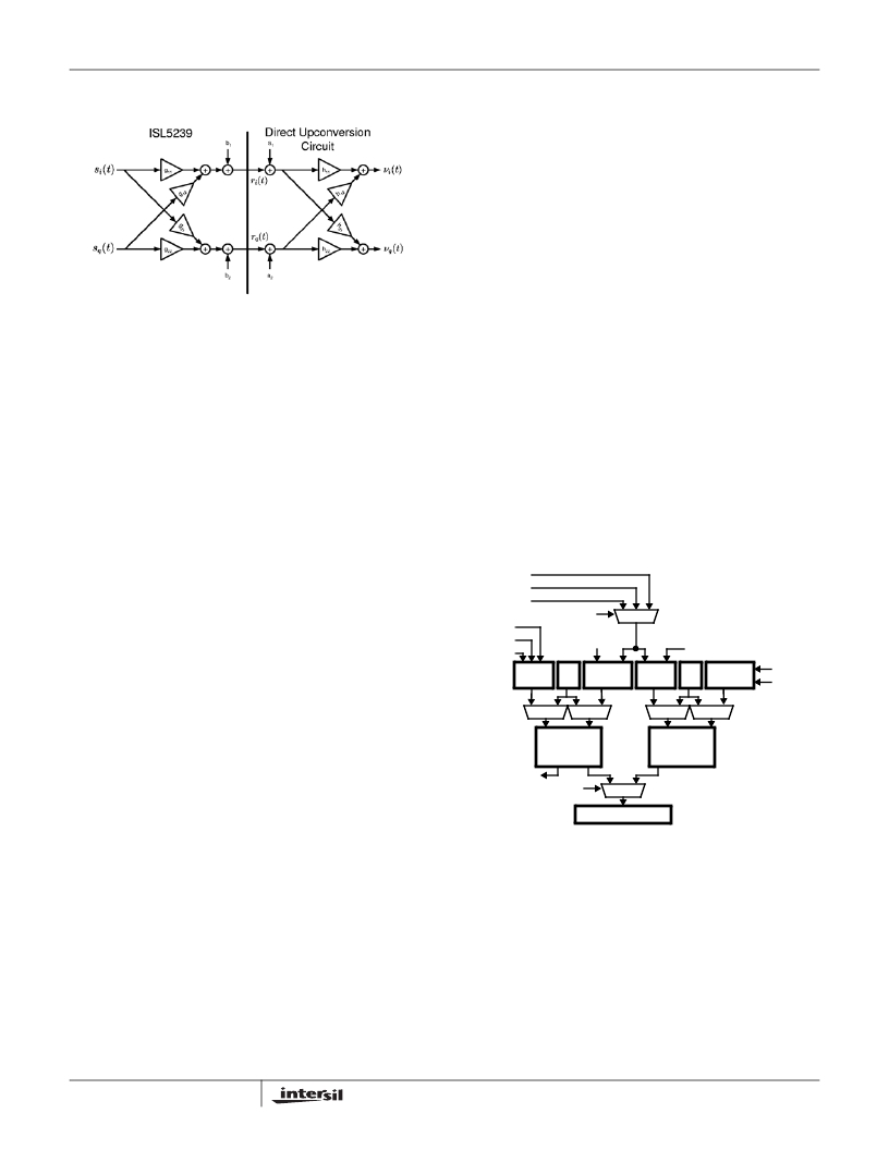
�ISL5239�
�cross-coupled� term� on� both� the� I� and� Q� channels.� Typical�
�implementation� is� as� shown� in� Figure� 10.�
�FIGURE� 11.� IMBALANCE� CORRECTION�
�The� Output� formatter� also� provides� DC� offset� correction� to�
�1/4� LSB� for� 18-bit� outputs� to� reduce� analog� DC� offsets�
�introduced� in� external� D/A� conversion� and� modulation�
�circuits� which� can� degrade� system� performance� by� causing�
�carrier� feed� through� in� complex� baseband� systems,� or� spurs�
�at� DC� for� IF� systems.�
�The� ODC� also� provides� programmable� output� precision� 8� to�
�18-bits,� with� unbiased� (convergent)� rounding,� since� practical�
�system� designs� will� require� D/A� converters� with� fewer� than�
�18-bits.� Internal� accuracy� is� in� excess� of� 18-bits,� and� utilizes�
�20-bit� data� paths� in� critical� areas.� Additionally,� both� two’s�
�complement� and� offset� binary� formats� are� supported.�
�Capture� Memory� (CM)�
�Feedback� Memory�
�The� feedback� memory� allows� the� user� to� capture� data� from�
�an� external� system� and� to� view� the� memory� through� the�
�processor� interface.� The� feedback� memory� is� used� to�
�observe� the� signals� coming� out� of� the� amplifier.� The� 1K� deep�
�memory� grabs� 20-bit� data,� either� in� parallel� or� serial� format.�
�The� feedback� capture� memory� has� its� own� clock� input,�
�FBCLK,� which� must� be� synchronously� derived� from� CLK� and�
�meet� the� timing� requirements.�
�Capture� operations� may� be� triggered� by� an� external� signal�
�(TRIGIN),� by� magnitude� threshold� crossings� detection�
�programmed� in� the� magnitude� threshold� maximum� and�
�minimum� values,� or� by� system� software� writing� to� the�
�processor� trigger� bit� in� control� word� 0x04,� bit� 6.� Separate�
�programmable� delays� of� up� to� 32k� samples� are� provided� for�
�both� input� memory� and� feedback� capture,� allowing� system�
�delays� to� be� calibrated� out� for� optimum� alignment� prior� to�
�analysis.� A� TRIGOUT� output� is� provided� to� indicates� when� a�
�capture� operation� has� begun.�
�The� processor� interface� to� the� capture� memories� is� designed�
�to� minimize� the� time� required� for� loading/unloading.� Although�
�access� to� the� memories� takes� place� through� indirect� address�
�and� data� registers,� auto� incrementing� of� the� address� is�
�supported� so� the� address� only� needs� to� be� written� once� to�
�access� the� entire� memory.� The� capture� memory� is� as� shown�
�in� Figure� 13.�
�TRIGIN�
�MAG� COMP�
�uP�
�The� Capture� Memory� allows� the� capture� and� viewing� of� data�
�TRIG� SEL�
�TRIG�
�from� various� points� in� the� chip.� The� primary� function� is� to�
�capture� the� digital� signals� coming� into� the� pre-distorter.� The�
�IFC� I,Q�
�PD� I,Q�
�PD� MAG�
�INPUT� DELAY�
�COUNT�
�FB� DELAY� COUNT�
�CM� also� provides� a� secondary� mode,� as� it� can� provide�
�stimulus� directly� to� the� pre-Distorter.� The� CM� is� comprised� of�
�INPUT�
�SEL�
�uP�
�INPUT�
�STATE�
�FB�
�STATE�
�uP� FORMAT�
�FBCLK�
�FB<19:0>�
�both� the� Input� and� the� Feedback� Memories.� The� processor�
�interface� provides� the� access� to� view,� input,� and� alter� the�
�DATA�
�ADDR�
�ADDR�
�DATA�
�memory� data.� Synchronized� (triggered)� capture� of� both� input�
�and� feedback� signals� is� a� typical� requirement� of� adaptive�
�INPUT�
�CAPTURE�
�MEMORY� 2K�
�FEEDBACK�
�CAPTURE�
�MEMORY� 1K�
�digital� pre-distortion� systems.�
�Input� Memory�
�The� input� capture� memory� observes� the� signals� going� into�
�the� amplifier.� The� 2K� deep� memory� grabs� complex� samples�
�of� data� at� one� of� three� possible� locations,� either� at� the� input�
�to� the� pre-distorter,� the� output� of� the� pre-distorter,� or� from� its�
�magnitude� calculation.� In� addition� to� capturing� input� data,�
�this� memory� may� also� be� configured� as� a� data� source.� The�
�input� capture� memory� may� be� pre-loaded� with� user� defined�
�data� and� ‘played’� into� the� pre-distorter� to� stimulate� the�
�system� with� signals� that� will� elicit� a� desired� response.�
�CM� TEST� I,Q�
�MEMORY� SELECT�
�uP� INTERFACE�
�FIGURE� 12.� CAPTURE� MEMORY� BLOCK� DIAGRAM�
�Memory� Modes� and� Programming� Instructions�
�Unless� noted,� the� following� discussion� applies� to� both� the�
�input� memory� and� feedback� memory� operations.� Prior� to�
�invoking� the� memory� to� capture� or� send� data,� the� control�
�word� 0x06,� bits� 14:0� input� trigger� delay� counter,� 0x08� bits�
�14:0� feedback� trigger� delay� count,� 0x05,� bits� 10:0� input�
�length,� 0x04,� bits� 2:1� input� memory� datain� source� or� 0x04,�
�bit� 8� feedback� input� format,� and� 0x04,� bits� 5:4� trigger� select�
�registers� must� be� loaded.�
�10�
�发布紧急采购,3分钟左右您将得到回复。
相关PDF资料
ISL5416EVAL1
EVALUATION PLATFORM FOR ISL5416
ISL55005IEZ-T7
IC AMP MMIC BIPO BROADBND SC70-6
ISL55007IEZ-T7
IC AMP MMIC BIPO BROADBND SC70-6
ISL55008IEZ-T7
IC AMP MMIC BIPO BROADBND SC70-6
ISL55009IEZ-T7
IC AMP MMIC BIPO BROADBND SC70-6
ISL55010IEZ-T7
IC AMP MMIC BIPO BROADBND SC70-6
ISL55011IEZ-T7
IC AMP MMIC BIPO BROADBND SC70-6
ISL55012IEZ-T7
IC AMP MMIC BIPO BROADBND SC70-6
相关代理商/技术参数
ISL5314
制造商:INTERSIL 制造商全称:Intersil Corporation 功能描述:Direct Digital Synthesizer
ISL5314_05
制造商:INTERSIL 制造商全称:Intersil Corporation 功能描述:Direct Digital Synthesizer
ISL5314EVAL2
制造商:Intersil Corporation 功能描述:DEV TOOL FOR COMMLINK DIRECT DGTL SYNTHESIZER - Bulk
ISL5314IN
功能描述:IC SYNTHESIZER DIGITAL 48-MQFP RoHS:否 类别:集成电路 (IC) >> 接口 - 直接数字合成 (DDS) 系列:- 产品变化通告:Product Discontinuance 27/Oct/2011 标准包装:2,500 系列:- 分辨率(位):10 b 主 fclk:25MHz 调节字宽(位):32 b 电源电压:2.97 V ~ 5.5 V 工作温度:-40°C ~ 85°C 安装类型:表面贴装 封装/外壳:16-TSSOP(0.173",4.40mm 宽) 供应商设备封装:16-TSSOP 包装:带卷 (TR)
ISL5314INZ
功能描述:IC SYNTHESIZER DIGITAL 48-MQFP RoHS:是 类别:集成电路 (IC) >> 接口 - 直接数字合成 (DDS) 系列:- 产品变化通告:Product Discontinuance 27/Oct/2011 标准包装:2,500 系列:- 分辨率(位):10 b 主 fclk:25MHz 调节字宽(位):32 b 电源电压:2.97 V ~ 5.5 V 工作温度:-40°C ~ 85°C 安装类型:表面贴装 封装/外壳:16-TSSOP(0.173",4.40mm 宽) 供应商设备封装:16-TSSOP 包装:带卷 (TR)
ISL54000
制造商:INTERSIL 制造商全称:Intersil Corporation 功能描述:Integrated Audio Amplifier Systems
ISL54000IRTZ
功能描述:IC AMP AUDIO PWR 1.23W AB 20TQFN RoHS:是 类别:集成电路 (IC) >> 线性 - 音頻放大器 系列:- 产品培训模块:Lead (SnPb) Finish for COTS
Obsolescence Mitigation Program 标准包装:2,500 系列:DirectDrive® 类型:D 类 输出类型:1-通道(单声道),带立体声耳机 在某负载时最大输出功率 x 通道数量:930mW x 1 @ 8 欧姆; 40mW x 2 @ 16 欧姆 电源电压:2.7 V ~ 5.5 V 特点:消除爆音,差分输入,I²C,静音,关闭,音量控制 安装类型:表面贴装 供应商设备封装:25-WLP(2.09x2.09) 封装/外壳:25-WFBGA,WLCSP 包装:带卷 (TR) 其它名称:MAX97000EWA+T-ND
ISL54000IRTZ-T
功能描述:IC AMP AUDIO PWR 1.23W AB 20TQFN RoHS:是 类别:集成电路 (IC) >> 线性 - 音頻放大器 系列:- 产品培训模块:Lead (SnPb) Finish for COTS
Obsolescence Mitigation Program 标准包装:2,500 系列:DirectDrive® 类型:D 类 输出类型:1-通道(单声道),带立体声耳机 在某负载时最大输出功率 x 通道数量:930mW x 1 @ 8 欧姆; 40mW x 2 @ 16 欧姆 电源电压:2.7 V ~ 5.5 V 特点:消除爆音,差分输入,I²C,静音,关闭,音量控制 安装类型:表面贴装 供应商设备封装:25-WLP(2.09x2.09) 封装/外壳:25-WFBGA,WLCSP 包装:带卷 (TR) 其它名称:MAX97000EWA+T-ND